◆ Features
Rated working voltage 4.5 V ~ 24 V, the limit voltages as low as 3.5 V;
Operating temperature range: -55℃ ~ 150℃;
Rated output current(sink) : 25 mA, the maximum output current(sink): 50 mA;
Switch response time is about 1μs, the operating frequency DC ~ 100 kHz;
Small temperature drift between operating point and release point;
No mechanical contact, no spark, switch signal stability, no shaking moment, high reliability and safety;
Products meet the EU RoHS instruction 2011/65 / EU and REACH regulations 1907/2006 / EU requirements.
◆ Outline
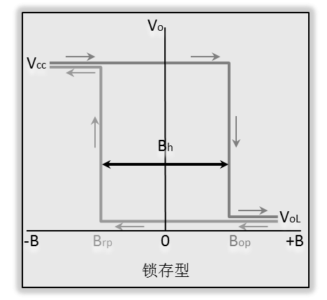
When the S pole of magnet faces the mark surface of the sensor and is closed to sensor(B≥Bop),the sensor outputs low level; When the N pole faces the mark surface and is closed to sensor (B≤Brp),the sensor outputs high level. When the magnet is far away with the sensor (B=0), the output status of the sensor is latched and keeps constant. In order to change the output status, the applied magnetic field must be opposite polarity. The magnet and electric transfer characteristic curve of AH513 is shown as the figure:

◆ 功能框图

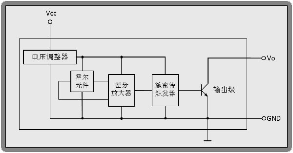
Hall sensor AH513 is one of bipolar excitation single-ended digital output Hall IC. The output signal owns latch function. The sensor chip has built-in reverse voltage protection, voltage regulators, temperature compensation circuit, Hall-voltage generator, signal amplifier, Schmitt trigger and open collector output drives circuit unit. Excellent voltage regulator and temperature compensation circuit ensure the sensor stable operates over a wide voltage range and temperature range, and the reverse voltage protection circuit avoids the sensor to be damaged by reverse voltage.
◆ Limit Parameter
| 参数 | 符号 | 最小值 | 最大值 | 单位 |
| 贮存温度 | Ts | -55 | 175 | ℃ |
| 电源电压 | VCC | 3.5 | 28 | V |
| 输出截止电压 | VO(off) | — | 300 | mW |
| 磁感应强度 | B | 不限 | 不限 | mT |
| 输出电流 | IO | — | 50 | mA |
◆静电等级
人体模式下,静电耐压大于±6kV。
◆工作条件
| 参数 | 符号 | 最小值 | 最大值 | 单位 |
| 电源电压 | VCC | 4.5 | 24 | V |
| 工作温度 | Ta | -55 | 150 | ℃ |
| 输出电流 | IO | — | 8 | mA |
◆电特性
| 参数 | 符号 | 测试条件 | 典型值 | 最大值 | 单位 |
| 输出低电平 | VOL | VCC1=4.5, VCC2=24V, IO=25mA, B≥BOP | 0.2 | 0.4 | V |
| 输出高电平 | VOH | VCC1=4.5, VCC2=24V, IO=25mA, B≤BRP | 23.5 | 24 | V |
| 输出漏电流 | IOH | VCC2=24V,VCC1开路 | 0.1 | 10 | μA |
| 电源电流 | ICC | VCC1=24V,Vo开路 | 3.5 | 8 | mA |
| 输出上升沿时间 | tR | VCC1=VCC2=12V,RL=1.2kΩ, CL=20pF | 125 | 150 | μs |
| 输出上升沿时间 | tF | 60 | 80 | μs |
◆磁参数
实验条件:VCC1 = VCC2 =24V,IO = 50mA
| 参 数 | 符号 | 最小值 | 典型值 | 最大值 |
| 工作点 | BOP | — | 4 | 7 |
| 释放点 | BRP | -7 | -4 | — |
| 回差︱工作点-释放点︱ | BH︱BOP-BRP︱ | 4 | 8 | 14 |
注1:单位为毫特斯拉, 1mT(毫特斯拉)=10Gs(高斯)。
注2:磁场S极垂直指向产品正面印记时,定义该磁场为B>0。
◆封装外形图
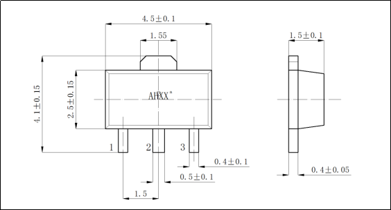
SOT-89封装图(单位为毫米)

注:封装外形图中,引脚1为Vcc,引脚2为GND,引脚3为输出端。
印记
印记XX或AHXX表示简称的产品型号。
Copyright © Nanjing AH Electronic Science & Technology Co., Ltd. All Rights Reserved.
Technical Support:  | Sitemap | Privacy Policy