◆ Features
Rated working voltage 4.5 V ~ 24 V, the limit voltages as low as 3.5 V;
Operating temperature range: -55℃ ~ 150℃;
Rated output current(sink) : 25 mA, the maximum output current(sink): 50 mA;
Switch response time is about 1μs, the operating frequency DC ~ 100 kHz;
Small temperature drift between operating point and release point;
No mechanical contact, no spark, switch signal stability, no shaking moment, high reliability and safety;
Products meet the EU RoHS instruction 2011/65 / EU and REACH regulations 1907/2006 / EU requirements.
◆ Outline
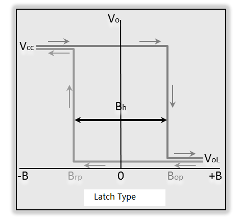
When the S pole of magnet faces the mark surface of the sensor and is closed to sensor(B≥Bop), the sensor outputs low level; When the N pole faces the mark surface and is closed to sensor (B≤Brp),the sensor outputs high level. When the magnet if far away with the sensor (B=0), the output status of the sensor is latched and keep constant. In order to change the output status, the applied magnetic field must be opposite polarity. The magnet and electric transfer characteristic curve of AH413 is shown as the figure:

◆ Block Diagram

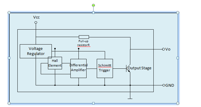
AH413 Hall sensor is one of bipolar excitation single-ended digital output Hall IC. The output signal owns latch function. The sensor chip has built-in reverse voltage protection, voltage regulators, temperature compensation circuit, Hall-voltage generator, signal amplifier, Schmitt trigger and open collector output drives circuit unit. Excellent voltage regulator and temperature compensation circuit ensure the sensor stable operates over a wide voltage range and temperature range, and the reverse voltage protection circuit avoids the sensor to be damaged by reverse voltage.
◆ Limit Parameter
| Parameter | Symbol | Min. | Max. | Unit | |||||
| Supply Voltage | VCC | 4.5 | 24 | V | |||||
| Operating Temp. | Ta | -55 | 150 | ℃ | |||||
| Output Current | IO | — | 8 | mA | |||||
| ◆ Electrical Characteristic | |||||||||
| Parameter | Symbol | Test Condition | Typ. Max. | Max. | Unit | ||||
| Output Low level | VOL | VCC1=4.5, VCC2=24V, IO=25mA,B≥BOP | 0.2 | 0.4 | V | ||||
| Output High Level | VOH | VCC1=4.5, VCC2=24V, IO=25mA,B≤BRP | 23.5 | 24 | V | ||||
Output Leakage Current | IOH | VCC2=24V,VCC1 Open circuit | 0.1 | 10 | μA | ||||
| Supply Current | ICC | VCC1=24V,Vo Open circuit | 3.5 | 8 | mA | ||||
Output Rise edge Time | tR | VCC1=VCC2=12V, RL=1.2kΩ, CL=20pF | 125 | 150 | ns | ||||
Output Fall Edge Time | tF | 60 | 80 | ns | |||||
◆ Magnetic Characteristic
Test condition:VCC1 = VCC2 =24V,IO = 50mA
| Parameter | Simbol | Min. | Typ. | Max. |
| Operate Point | BOP | — | 4 | 7 |
| Release Point | BRP | -7 | -4 | — |
| Hysteresis ∣Operate point –Release Point∣ | BH ∣BOP-BRP ∣ | 4 | 8 | 14 |
Note 1: Unit : mt, 1mt=10Gs.
◆ Package Outline
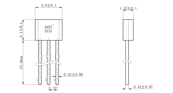
TO-92UA/TO-92S Package figure(Unit: mm)

Note: In the package outline, Pin1 is Vcc, Pin 2: GND, Pin3: output terminal.
Mark
Mark “XX”or “AHXX” are abbreviation form of parts No.
Copyright © Nanjing AH Electronic Science & Technology Co., Ltd. All Rights Reserved.
Technical Support:  | Sitemap | Privacy Policy